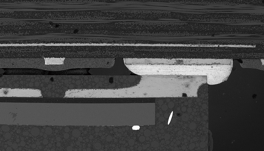
SEM can be used for microscopic morphology observation, cross-section preparation, defect analysis, and failure analysis of printed circuit boards (PCBs) and flexible printed circuit boards (FPCs). It can inspect the surface morphology and adhesion between copper foil and resin substrates, dry film adhesion and detachment, and the degree of nickel corrosion, and rapidly measure intermetallic compound (IMC) layer thickness to evaluate soldering reliability. For complex structures such as multilayer boards, blind vias, and buried vias, combined with ion beam milling, it enables cross-section preparation and internal defect localization, solving the problems of traditional cross-sectioning, such as high destructiveness and difficulty in compositional analysis.
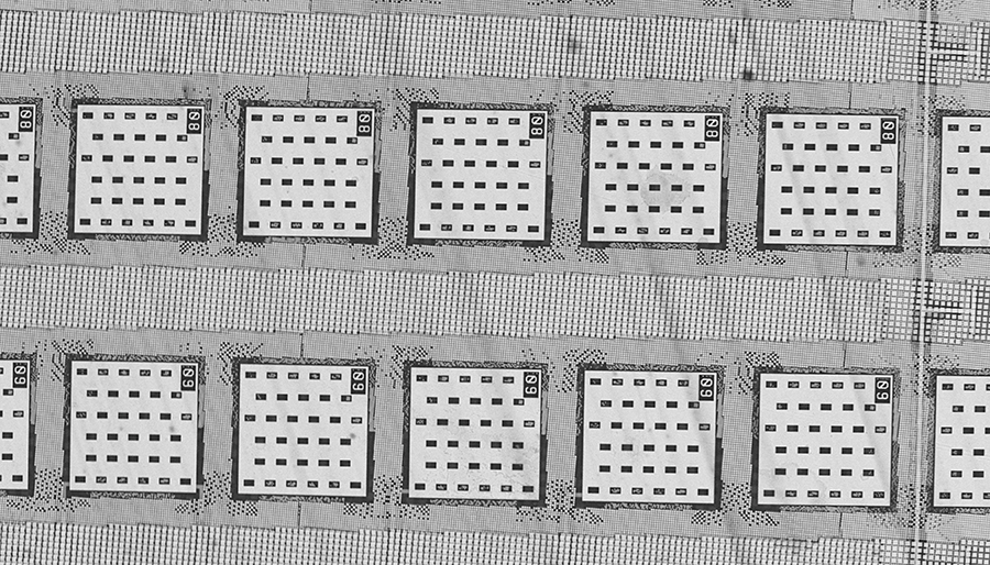
In front-end-of-line (FEOL) chip manufacturing processes, scanning electron microscopy (SEM) is widely used for quality inspection and process diagnostics in key steps such as lithography, etching, and thin-film deposition. It can detect open circuits, short circuits, and bridging in interconnects, as well as pattern defects from lithography and etching processes. It can evaluate film thickness, coverage quality, and step coverage, and accurately determine the position and depth of PN junctions. For advanced transistor structures such as FinFETs and gate-all-around (GAA) devices, high-resolution imaging enables the characterization of nanometer-scale feature sizes.
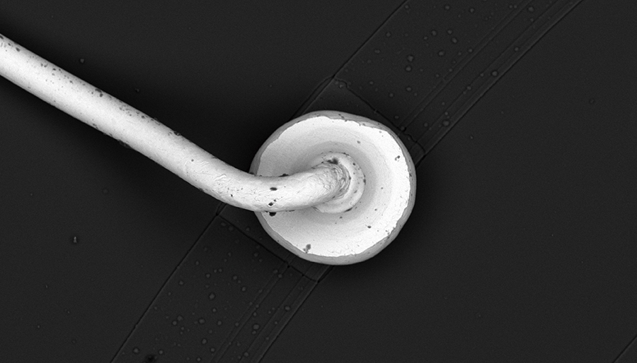
For various discrete devices, passive components, and assembled electronic components, scanning electron microscopy (SEM) is commonly used for failure analysis and quality control. High-resolution imaging can identify microscopic defects such as open circuits, short circuits, and bridging in metallization layers. In combination with voltage contrast imaging, it can diagnose latch-up effects in CMOS circuits and leakage paths in PN junctions. For thermistors, ferroelectric materials, passivation layers, and other materials, SEM can also be used to observe grain size, particle distribution, and microstructure, providing a basis for device performance optimization and fabrication process improvement.
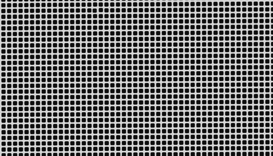
SEM is widely used in semiconductor wafer defect inspection, critical dimension measurement, and defect review and classification after final CP testing. Electron beam defect review equipment can acquire high-resolution morphological images of wafer surface defects. Relying on deep learning-driven automatic defect recognition and classification algorithms, it achieves intelligent detection and classification of hotspot defects. At the same time, it can accurately measure the linewidth and pattern profile dimensions of multilayer thin-film structures on wafers and locate process anomalies, providing intuitive microscopic evidence and quantitative data support for process optimization and chip yield improvement.


