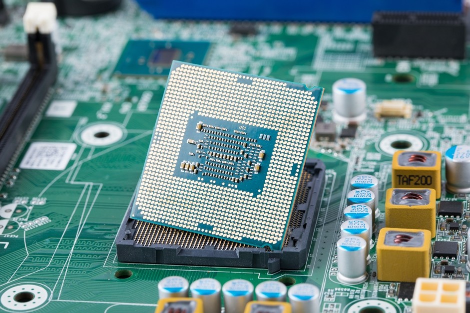
With the continuous progress of science and technology, the quality control of the internal PCB board is becoming more and more strict, and then the development and upgrade of PCB surface treatment technology is becoming more and more urgent. This paper introduces the surface treatment technology of PCB.
What is surface treatment
PCB surface treatment technology refers to the process of artificially forming a surface layer on PCB components and electrical connection points with mechanical, physical and chemical properties different from the substrate. The purpose is to ensure good solderability and electrical performance of PCB. Because copper tends to be present in the air as oxide, which seriously affects the solderability and electrical properties of the PCB, surface treatment of the PCB is required.

Common surface treatment
Organic oxidation protection (OSP)
OSP is a process for copper foil surface treatment of printed circuit boards (PCB) in accordance with the RoHS directive. OSP is short for Organic Solderability Preservatives, also known as Organic Solderability Preservatives or Preflux in English. Simply put, OSP is the chemical growth of an organic skin film on a clean, bare copper surface.
This film has anti-oxidation, heat shock resistance, moisture resistance, to protect the copper surface in the normal environment no longer continue to rust (oxidation or vulcanization, etc.); However, in subsequent welding at high temperatures, this protective film must be easily and quickly removed by the flux, so that the exposed clean copper surface can be immediately combined with the molten solder into a solid solder spot in a very short time.
Hot air leveling
Hot air leveling, also known as hot air welding leveling (commonly known as tin spraying), is a process of coating the PCB surface with molten tin (lead) solder and heating compressed air leveling (blowing) to form a coating layer that is not only resistant to copper oxidation, but also provides good solderability. Hot air finishing solder and copper form intermetallic cu-tin compounds at the junction. PCB for hot air conditioning to sink in molten solder; Air knife blows liquid solder flat before solder solidifies; Wind knife minimizes meniscus of solder on copper surface and prevents solder bridging.
Zedoary
Zedoary is a thick layer of nickel gold alloy with good electrical properties wrapped on the copper surface, which can protect the PCB for a long time. It also has a tolerance to the environment that no other surface treatment process has. In addition, the gold can also prevent the dissolution of copper, which will benefit lead-free assembly.
Its advantages are not easy to oxidize, can be stored for a long time, the surface is smooth, suitable for welding pin clearance and small solder joint components. Preferred PCB board with key (e.g. mobile phone board). Reflow soldering can be repeated many times without much loss of solderability. It can be used as the base material for COB (Chip On Board) cabling.
Its disadvantages are high cost, poor welding strength, because of the use of nickelless plating process, easy to have the problem of black disk. The nickel layer oxidizes over time and has no long-term reliability.
Silver coat
Between OSP and electroless nickel plating/gold leaching, the process is simple and fast. Still provides good electrical properties and maintains good solderability but loses luster when exposed to heat, humidity and pollution. Since there is no nickel underneath the silver layer, silver coat does not have the good physical strength of electroless nickel plating/gold leaching.
Tin coat
PCB tin deposition process is specially designed for SMT and chip packaging by chemical deposition of tin metal coating on copper surface. It is a new green and environmental protection process to replace PB-Sn alloy coating process. It has been widely used in electronic products (such as circuit boards, electronic components), hardware, decoration and other surface treatment.
Nickel and gold
(1) chemical precipitation of nickel gold
The copper surface is coated with a thick layer of nickel gold alloy with good electrical properties and can protect the PCB for a long time. Unlike OSP, which is only used as a rust barrier, it can achieve good electrical performance in the long-term use of PCB. In addition, it also has a tolerance to the environment that other surface treatment processes do not have;
(2) Electroplating nickel gold
A layer of nickel is first plated on the surface conductor of PCB and then a layer of gold is plated. The main purpose of nickel plating is to prevent the diffusion between gold and copper. There are two types of nickel gold plating: soft gold plating and hard gold plating. Soft gold is mainly used for chip packaging gold line; Hard gold is mainly used for electrical interconnections in non-welded areas.
Tin
(1) lead spray tin
The so-called lead spray tin refers to the tin according to a certain proportion, modulation, lead will improve tin wire activity in the welding process, lead tin wire is relatively better than lead-free tin wire, but lead is toxic, lead in lead is harmful to human body; The eutectic temperature with lead is lower than that without lead. The specific amount depends on the composition of the lead-free alloy, such as SNAGCU eutectic temperature is 217 degrees, welding temperature is eutectic temperature plus 30~50 degrees. It depends on the actual adjustment. Lead eutectic is 183 degrees. Mechanical strength, brightness, etc. with lead is better than without lead. Therefore, lead tin is not environmental protection, and the world's environmental protection has a certain difference. Thus, lead-free tin spray was born.
(2) lead-free tin spraying
Lead-free tin is a kind of environmental protection process, it is very small harm to human body, is also a kind of process advocated at this stage, lead-free tin for lead content is not more than 0.5, lead-free tin will have a high melting point, so that the welding point is much stronger. In essence, tin-spraying with lead and tin-spraying without lead is a process. It's just the purity of the lead is different. Lead-free tin is more environmentally friendly and safer for the human body and the environment. It is also a development trend in the future. It is recommended to use it.
PCB hybrid surface treatment technology
Choose two or more than two kinds of surface treatment methods for surface treatment, the common forms are: nickel immersion gold + oxidation prevention, nickel plating gold + nickel immersion gold, nickel plating gold + hot air leveling, nickel immersion gold + hot air leveling, lead-free tin spraying + gold finger.
Product recommendations
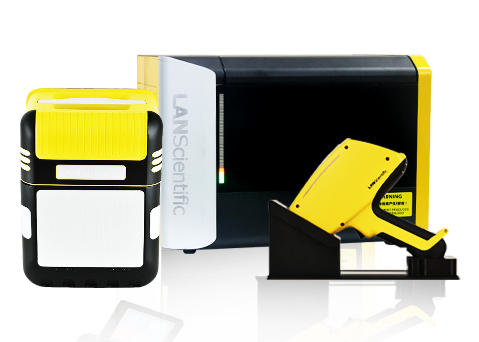
For PCB surface treatment process control, product quality inspection and other links of detection and screening problems, LANScientific provides you with efficient XRF analysis solutions, including a series of products: Handheld, portable and benchtop XRF instruments provide fast, efficient, nondestructive and accurate analysis of PCB surface treatment thickness and composition to meet your different analysis purposes and needs.

